Homepage of Stefan Salewski
PetEd -- a simple electronics schematics editor
Preview -- October 2015
Although the tool is still unfinished and not really useful, I have decided to upload the source already to www.github.com/stefansalewski. A tar archive is available for download at the bottom of this page.
Development is currently done with Ruby 2.2, GTK 3.16 and Ruby-Gnome2 bindings 3.06 from git on Linux. Older Ruby GTK bindings may not work well -- git install as described at https://github.com/ruby-gnome2/ruby-gnome2 can be done without root provilegies on your linux box and installs in a .gem directory in your home directory. At a later point in time your Linux distribution should offer working bindings as well. (The tool may work on Windows or MacOS as well, maybe some fixes will be necessary.)
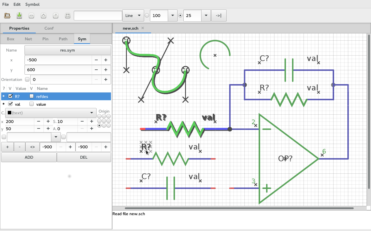
The purpose of this program is to provide a nice schematics editor compatible with the gschem tool of the gEDA software.
The editor should be easy to use, look nice and allow easy customisation (colors, fonts, line-with...) and offer high quality export to pdf, svg, png... The current implementation is written in Ruby and uses GTK3 user interface and Cairo drawing functions. Basically it is a Linux tool, but may work with other operating systems when GTK3 is available. The code is short (6k loc) and simple, so user level customisation and extension or a later port to a compiled language like Vala, Rust or Nim for more speed should be not a big task. (We should not expect a very large performance increase when using a compiled language because a large part of CPU power is consumed by Cairo's drawing routines itself. I am expecting only a factor two -- for more we may need multi-treading or OpenGl support.)
(I know that some people wants a schematics editor for tablets. Unfortunately a nice user interface for desktop use with mouse is very different from tablet input behavior, and there is currently no GTK support for Android tables. So there is currently no plan in that direction.)
The largest part of the code was written in 2012, in 2014 I did some cleanup and some small extensions. Basically the code is working already, but more cleanup is necessary, and we have to add some more functionality. All that is easy, but not really interesting...
Hardware Requirements
The program is best used with a 3 keys computer mouse preferable with scroll wheel. A color display with at least full hd resolution is useful. Using a notebook without a mouse should work, but makes operation less enjoyable. Nearly all basic operations can be done with the mouse, but for text input a keyboard should be available. Some actions like CANCEL or DELETE may be available from the keyboard too, and SHIFT and CONTROL keys may work as modifiers for mouse actions.Software Requirements
Ruby 2.0+GTK3
Cairo
Generally we use Linux, but other operating systems may work also.
Installation
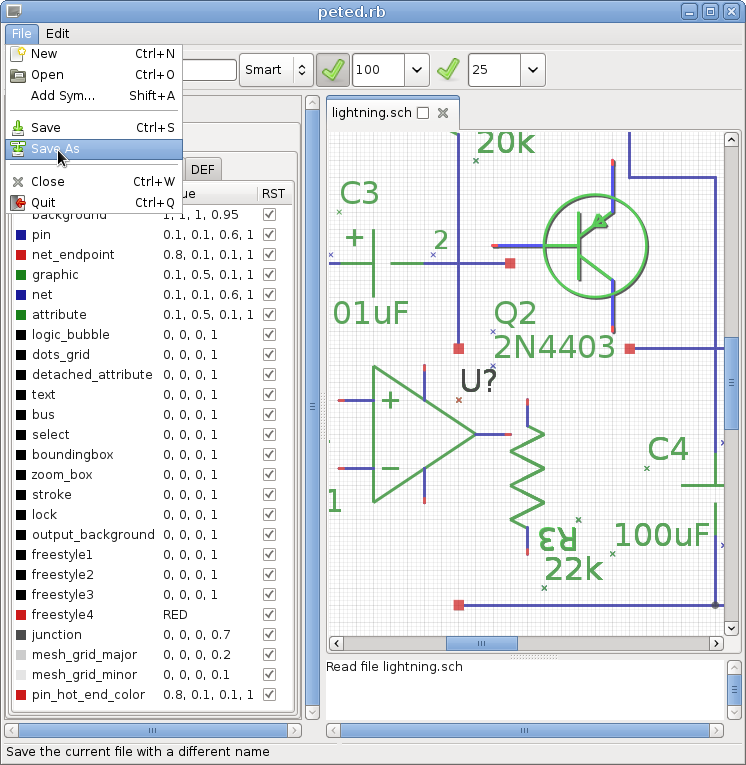
Extract the tar achieve somewhere in your home directory, cd into that directory and type 'ruby peted.rb test.sch' to launch the application from inside your shell (terminal) window.Currently I can not provide install scripts like Ruby gem files.
Most people will use this program together with the gEDA package and associated software like PCB layout program or gnucap simulator. Using it without installed gEDA package is possible, but then the symbol set is really small (empty currently) and tools like gnetlist for netlist export are not available.
Usage
You may start the program with the command "ruby peted.rb test.sch" from the command line. That may fail if it can not find symbols -- that is if gEDA is not installed or if Symbols are installed somewhere other. We will fix that later. If it fails, you may try starting the program without argument, that should open an empty window.Currently we have a drawing area for the schematics, a properties and configuration area at the left and an area for message logging at the bottom. The areas use panels for resize and tabulator buttons at the top for switching displayed content.
One important goal of user interface design was to make tool switching nearly unnecessary -- all basic operations are available always and with minimal effort, generally only with the mouse without touching the keyboard. Most actions in the drawing area are done with the mouse and depends on the location of the mouse pointer: If at least one elements is selected and pointer is over a selected one, then the actions works on all the selected elements. When pointer is hovering over an unselected element, the actions works on this one. And finally, when pointer is over an empty area of the schematic, then other, more general actions are provided.
The two most basic mouse actions are 'hit' and 'drag'. 'hit' means pressing and releasing a button without moving the mouse, 'drag' includes some movement in the action sequence. We use the abbreviation LMB, MMB and RMB for left, middle and right mouse buttons. Mouse actions vary for mouse position, i.e. mouse pointer over an empty area, centered over an element, or hovering over a special location, i.e. pin or net endpoint.
Generally it should be easy to discover the available actions: LMB 'hit' is mostly used for selecting or unselecting elements. Hit over element selects it, hit over empty area unselects all selected elements (Currently unselect works in two levels for elements with attached attributes -- first selected attributes are unselected, after that the element is unselected itself.). If no element is selected, then a LMB hit over an empty area starts a new element -- the type of new element (net, line, text...) is selected by a box widget at the top of the main window. Hit select operation can be modified with SHIFT and CONTROL keys held down -- add to selection, remove from selection and toggle. Some elements are smart, so LMB hit on net or pin endpoint should always start a new net. Hit on a line endpoint starts a new line with inheritated color and line width.
Drag-operations started with LMB over an elements moves it (it is not necessary to select it). If multiple elements are selected and you move one of them, then all other selected ones are moved also. Textual attached attributes of elements build their own group, so if they are selected and you move one, other selected ones from that group follow, but other objects not. Some elements are smart, so when you move the center of a net segment, then the whole elements will move, but when you move one end, then only that end moves. Generally all elements under the mouse pointer are moved at once -- you may press LMB multiple times to select only one. A LMB drag started over an empty area draws a selection rectangle -- you can enforce this by pressing SHIFT key modifier when drag action starts. Add to selection, toggle or unselect is available with SHIFT and CONTROL key modifiers held down when LMB is released.
Drag-like operation with MMB can be used for panning when started over an object, or for zoom into a rectangle when starting over a void area. (If you really need it, use CONTROL or SHIFT key modifier to switch this behavior). Some objects may support a MMB hit operation, i.e. this can be used to divide a net segments into two pieces.
With the scroll wheel you can rotate objects around the current mouse pointer position when elements are selected or the mouse pointer hovers over an element, or it does zooming when pointer is over a void area.
The RMB generally opens a context sensitive popup menu with some basic operations. Additional some keyboard support it available -- 'm' key starts moving objects, 'd' may work for delete operation. But we don't really need keyboard for this.
Grid
We have two grids controlled by the boxes at the top. You can select grid size for both, and use the button to select the active (snap) grid. So fast switching between width and narrow grid is available. Object types We have graphic elements like lines, boxes, circles, paths and the electrically elements pins and nets. Pins together with the graphical elements can be grouped to symbols like a resistor or OpAmp symbol, stored separately with .sym file extension. All objects can have attached textual attributes (properties) of the form 'name=value', both substrings may be invisible. For pins this is generally something like name, number or sequence. Symbols generally have attributes like RefDes (Reference Designator), Value (100k for resistor) and footprint (land pattern for PCB layout). For symbols we have the special case, that some attributes may be stored in the symbol files when the symbols was created, and other attributes are added or replaced when the symbol is included in the schematic. Attributes are processed when the schematic is imported into PCB program or other programs, or with gEDA's gnetlist tool to generate netlists and other files for special purposes.The object properties area
At the left there are some widgets which show properties of single selected elements. This includes basic data like location, color, line width and the attributes list, which generally is empty for pure graphical elements.Main Menu and Toolbar
We try to have only a small set of items which should not need explanations.Configuration Box
At the left, below the properties area, there is a list with all the configuration options. We have independent sets for screen and various exporters, with a common default. The RST checkbox is used to reset a value -- back to value stored in configuration file for the common defaults, or back to that common default for sets like PNG. Additional you can define named colors, which you then can reference by name. Colors have RGBA values with components ranging from 0 to 1 each. Currently a color value dialog is not available, it may be added later, but does not really offer a real benefit. Entering numbers works better. Currently configuration is not saved!Loading symbols
Currently we have no preview available and use the ordinary file dialog.Creating a Schematic
Generally you load and place the symbols and connect the pins with nets. And you add some attributes, i.e. unique RefDes (Reference Designator) for symbols and an footprint attribute which is used for PCB import.Restrictions
Of course a lot functionality is curently not working as expected, but that should change during the current cleanup of the code. Busses, images and undo operation are currently unsupported intentionally, that will change in a later release.Related work:
- geda-project.org
- kicad-pcb.org
- fritzing.org
- qucs
- opencircuitdesign
- aacircuit
- wedana (HTML5 gschem clone)
- PSchem (Python gschem clone)